Apr2017

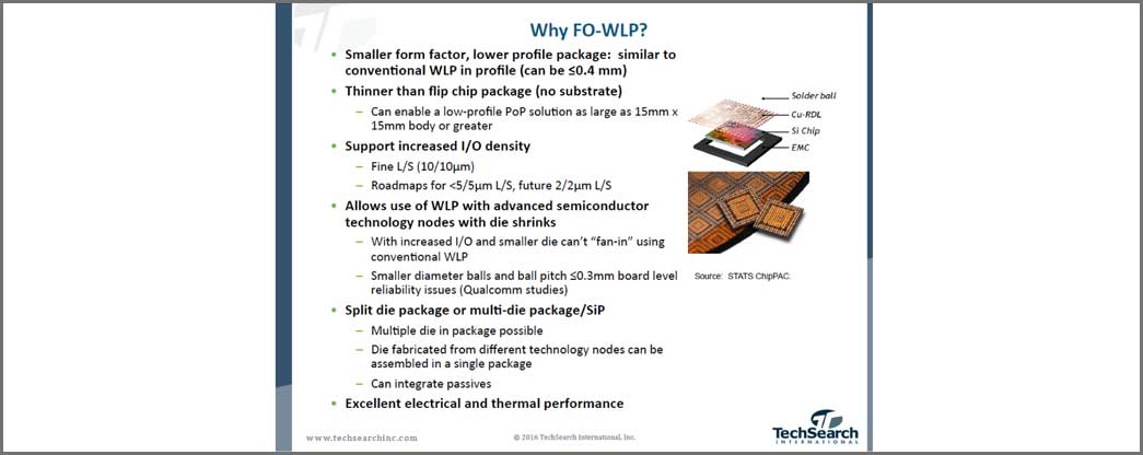
Fan-Out Wafer Level Packaging (FOWLP) has become the buzz word and hot topic for the semiconductor industry. As TechSearch International discussed at the recent SEMI Strategic Materials Conference, FOWLP offers numerous performance and cost advantages in terms of smaller form factor and thinner package, higher I/O density, multi-die solutions, and more. While FOWLP technology has been developed and discussed for years, only now we are certain that it will make a big splash in the market. This all comes from one of the world’s best-selling gadgets, the Apple iPhone.
Apple’s iPhones have always been a market trend setter by incorporating new features and technologies in their products and refreshing them every year. This year’s iPhone 7 brings in more than new cameras, faster processor, and high color gamut display. Inside the new iPhone 7, the 16nm FinFET-based A10 processor has implemented TSMC’s FOWLP-based InFO (Integrated Fan-Out) technology integrating application processor and mobile DRAM in one package. What sets the FOWLP apart from package-on-package (POP) form factors found in earlier generations of iPhones are thinner packaging profile, higher I/O counts, better electrical and thermal performance, and yet a better cost structure. This is clearly a game changer of the packaging industry. Apple/TSMC have set the tone for the packaging technologies trend in mobile market in the years to come. Behind the success of InFO implementation in the iPhone, TSMC has been developing the technologies since 2014. To facilitate the commercialization, TSMC set up a new back-end facility in Longtan dedicated to advanced packaging technologies, which is also the production base for InFO. TSMC also plans to introduce second generation InFO technology along with the mass production of 10nm chips scheduled in 2017, while expanding its InFO production to its Taichung site. Meanwhile, leading OSATs are all following suit by building up FOWLP capabilities to defend their turf and to serve the rising demand, especially in mobile applications, for these packages. ASE Group is building a Fan-Out line in Kaohsiung targeting mass production in late 2016/early 2017; Amkor set up a FOWLP line in Korea; SPIL is going to deploy Fan-Out line in Taichung in 2017. Almost all other major OSATs, as well as some IDMs (Samsung, STMicroelectronics, and others), are planning their versions of fan-out packaging. The implementation of FOWLP is expected to impact related equipment and materials market in the years to come. TSMC spent almost 10% of their capex this year (US$ 9.5 billion) on InFO capacity. Though some of the investment is meant for 2017 capacity, it’s still a significant amount. The investment momentum will continue with OSATs and IDMs getting into the market. Related equipment segments including SMT placement equipment (pick and place), PVD, PECVD, ECD, and compression molding shall benefit most from the capacity build-up. On the material side, dielectric materials and new molding compounds are playing an important role in delivering a reliable and cost effective solution. And, the elimination of the package substrate and underfill during the FOWLP process will also have some impact on the respective markets. Going forward, we will see more FOWLP implementation in packaging baseband processors, PMIC, GPU, and RF devices in mobile devices and wearable products. FOWLP also has the potential extending to CPU, GPU, FPGA packaging for high-performance computing. As noted by TechSearch and other industry leaders, FOWLP is not only a disruptive technology but also changes the dynamics in the foundry-OSAT ecosystem. FOWLP is taking off and will be a form factor flexible enough to deliver solutions for heterogeneous integration needed in many emerging applications. For more information about SEMI, visit www.semi.org!
Shared May 1, 2017
